I have drawn up a schematic (click to enlarge) of the high current and sensing portions of my maximum power point tracking (MPPT) 2-phase boost converter battery charger circuit. The schematic does not include the micro-controller, MOSFET gate driver IC, and associated power supplies, as those items are on the (relatively) low-power side of things.
What do all of these things do?
- L1, Q1, and D1 – These three components make up the heart of the boost converter. When Q1 turns on, power builds up in L1 as the current rises. When Q1 turns off, all of that power exits via the only available route (out past D1) and the voltage is boosted as the inductor (L1) resists the current change. If you turn Q1 on and off very quickly (under control of the micro-controllers’ PWM output via a MOSFET gate driver) it raises the output voltage higher than the input voltage.
- L2,Q2 and D2 – See L1,Q1, and D1 above. These three guys act in the same way, but Q2 is turned on and off 180 degrees out of phase from Q1. So while one half of the circuit is drawing power in, the other half is pushing power out, and visa-versa. This doubles the power capacity of the circuit, and reduces the size of the filter capacitors that are needed, as they are shared between the two phases.
- C1 & C2 – Ceramic & Electrolytic capacitors that work together to filter the input power (i.e. they provide short bursts of current needed when Q1 or Q2 turn on)
- C3 & C4 – Ceramic & Electrolytic capacitors that work together to filter the output power (i.e. they absorb the short bursts of current leaving L1 and L2 when Q1 or Q2 turn off)
- R1, R2, and C5 – Voltage sensing. R1 and R2 are a classic voltage dividing resistor network. Because R1 is so much larger than R2, the high voltage output (up to 200 volts) is reduced to a low voltage output on the “VOLTAGE SENSE” output (between 0-5 volts), suitable for a microcontroller input (A2D) pin. Because it is coming out of a switching boost converter, the output voltage has a lot of noise in it, so capacitor C5 helps to reduce this. I still had to make multiple sense readings on the microcontroller input pin and average them to get a reliable reading. I expect that if I made an analog low-pass filter on the voltage sense output it could fix this with a higher component count.
- R3, U2, R4,R5, Q3 – These are the current sensing subsystem. R3 is a 0.1 ohm 5watt resistor that is acting as a current shunt. 1 amp flowing through this resistor equates to a 0.1 volt drop from one side of the resistor to the other. U2, the AD8212 chip amplifies this small voltage, and together with Q3, converts it to a low voltage signal suitable for a microcontroller A2D input pin. Currently R5 (at 100K) is set up for a 100x gain in the amplification, but I may reduce that as I start to test at higher power levels.
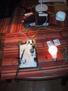
In reality, I have not yet soldered D2 and Q2 onto my pref-board, so the circuit is currently a single phase boost converter. This is fine, as I am not yet testing it at full power and my current microcontroller isn’t powerful enough to output a proper 2 phase control signal anyways. On the software side, I have gotten my micro-controller to regulate the circuit to output a (relatively) constant voltage regardless of the input voltage by controlling the PWM duty cycle. I have measured the current-sense output using a multi-meter and it is working, but I have not yet integrated current sensing into the control software. Here is a picture of the pref-board. The current sense module is still on a solder-less breadboard next to it.
My lack of progress on the software side is due to a lack of the proper development tool (PIC Kit 3) which is required to program the newer PIC microcontroller that I selected (PIC16f1824) to drive both phases of the boost converter. When I ordered the new PIC’s I didn’t read the specifications closely enough and just assumed that my eight year old PICKit1 would be able to program it. Silly me….Apparently Microchip has made some improvements in the last eight years. Of course, when I got the new chips, I ripped my code apart to make it work with the dual ECCP PWM modules and faster internal clock, and by the time I figured out that I couldn’t program the new chip I had already gotten the code to a state where I didn’t want to reverse all of my changes just to be able to play with the old microcontroller for a few days until the new programmer arrived. On the plus side, the new chip has an internally generated 32Mhz clock which will (eventually) let me run two PWM channels 180 degrees out of phase with a duty cycle of 125 kHz and 8 bits of resolution. It also has a UART, so I can easily use a serial LCD module for displaying status information.


I need boost converter dc to DC 12v to 80 or over out put and amp 3 min by mosfet.ic. coil
My ic no.uc3845